- 您现在的位置:买卖IC网 > Sheet目录3886 > PIC16C54C-04/SO (Microchip Technology)IC MCU OTP 512X12 18SOIC
PIC18F2450/4450
DS39760A-page 122
Advance Information
2006 Microchip Technology Inc.
12.2
Timer2 Interrupt
Timer2 also can generate an optional device interrupt.
The Timer2 output signal (TMR2 to PR2 match)
provides the input for the 4-bit output counter/
postscaler. This counter generates the TMR2 match
interrupt flag which is latched in TMR2IF (PIR1<1>).
The interrupt is enabled by setting the TMR2 Match
Interrupt Enable bit, TMR2IE (PIE1<1>).
A range of 16 postscale options (from 1:1 through 1:16
inclusive) can be selected with the postscaler control
bits, T2OUTPS3:T2OUTPS0 (T2CON<6:3>).
12.3
TMR2 Output
The unscaled output of TMR2 is available primarily to
the CCP module, where it is used as a time base for
operations in PWM mode.
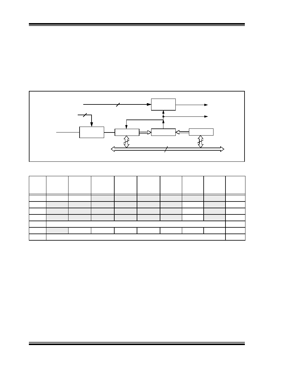
FIGURE 12-1:
TIMER2 BLOCK DIAGRAM
TABLE 12-1:
REGISTERS ASSOCIATED WITH TIMER2 AS A TIMER/COUNTER
Name
Bit 7
Bit 6
Bit 5
Bit 4
Bit 3
Bit 2
Bit 1
Bit 0
Reset
Values
on page
INTCON GIE/GIEH
PEIE/GIEL
TMR0IE
INT0IE
RBIE
TMR0IF
INT0IF
RBIF
PIR1
—
ADIF
RCIF
TXIF
—
CCP1IF
TMR2IF
TMR1IF
PIE1
—
ADIE
RCIE
TXIE
—
CCP1IE
TMR2IE
TMR1IE
IPR1
—
ADIP
RCIP
TXIP
—
CCP1IP
TMR2IP
TMR1IP
TMR2
Timer2 Register
T2CON
—
T2OUTPS3 T2OUTPS2 T2OUTPS1 T2OUTPS0 TMR2ON
T2CKPS1 T2CKPS0
PR2
Timer2 Period Register
Legend: — = unimplemented, read as ‘0’. Shaded cells are not used by the Timer2 module.
Comparator
TMR2 Output
TMR2
Postscaler
Prescaler
PR2
2
FOSC/4
1:1 to 1:16
1:1, 1:4, 1:16
4
T2OUTPS3:T2OUTPS0
T2CKPS1:T2CKPS0
Set TMR2IF
Internal Data Bus
8
Reset
TMR2/PR2
8
(to PWM)
Match
发布紧急采购,3分钟左右您将得到回复。
相关PDF资料
PIC16F722-I/ML
IC PIC MCU FLASH 2KX14 28-QFN
PIC16LCE623T-04I/SO
IC MCU CMOS.5K OTP W/EEPRM18SOIC
PIC16HV540-04I/SO
IC MCU OTP 512X12 18SOIC
PIC16LCE623T-04E/SS
IC MCU CMOS.5K OTP W/EEPRM20SSOP
PIC16LCE623T-04E/SO
IC MCU CMOS.5K OTP W/EEPRM18SOIC
5-520415-4
CONN TRIOMATE 4POS VERT TIN
6-176982-6
CONN TRIO-MATE 16POS .100 FFC
PIC16LCE623-04I/SO
IC MCU CMOS.5K OTP W/EEPRM18SOIC
相关代理商/技术参数
PIC16C54C-04/SO
制造商:Microchip Technology Inc 功能描述:8BIT CMOS MCU SMD 16C54 SOIC18
PIC16C54C-04/SO
制造商:Microchip Technology Inc 功能描述:Microcontroller IC Number of I/Os:12
PIC16C54C-04/SS
功能描述:8位微控制器 -MCU .75KB 25 RAM 12 I/O 4MHz SSOP20 RoHS:否 制造商:Silicon Labs 核心:8051 处理器系列:C8051F39x 数据总线宽度:8 bit 最大时钟频率:50 MHz 程序存储器大小:16 KB 数据 RAM 大小:1 KB 片上 ADC:Yes 工作电源电压:1.8 V to 3.6 V 工作温度范围:- 40 C to + 105 C 封装 / 箱体:QFN-20 安装风格:SMD/SMT
PIC16C54C-04E/P
功能描述:8位微控制器 -MCU .75KB 25 RAM 12 I/O 4MHz ExtTemp PDIP18 RoHS:否 制造商:Silicon Labs 核心:8051 处理器系列:C8051F39x 数据总线宽度:8 bit 最大时钟频率:50 MHz 程序存储器大小:16 KB 数据 RAM 大小:1 KB 片上 ADC:Yes 工作电源电压:1.8 V to 3.6 V 工作温度范围:- 40 C to + 105 C 封装 / 箱体:QFN-20 安装风格:SMD/SMT
PIC16C54C-04E/SO
功能描述:8位微控制器 -MCU .75KB 25 RAM 12 I/O 4MHz Ext Temp SOIC18 RoHS:否 制造商:Silicon Labs 核心:8051 处理器系列:C8051F39x 数据总线宽度:8 bit 最大时钟频率:50 MHz 程序存储器大小:16 KB 数据 RAM 大小:1 KB 片上 ADC:Yes 工作电源电压:1.8 V to 3.6 V 工作温度范围:- 40 C to + 105 C 封装 / 箱体:QFN-20 安装风格:SMD/SMT
PIC16C54C-04E/SS
功能描述:8位微控制器 -MCU .75KB 25 RAM 12 I/O 4MHz Ext Temp SSOP20 RoHS:否 制造商:Silicon Labs 核心:8051 处理器系列:C8051F39x 数据总线宽度:8 bit 最大时钟频率:50 MHz 程序存储器大小:16 KB 数据 RAM 大小:1 KB 片上 ADC:Yes 工作电源电压:1.8 V to 3.6 V 工作温度范围:- 40 C to + 105 C 封装 / 箱体:QFN-20 安装风格:SMD/SMT
PIC16C54C-04I/P
功能描述:8位微控制器 -MCU .75KB 25 RAM 12 I/O 4MHz IndTemp PDIP18 RoHS:否 制造商:Silicon Labs 核心:8051 处理器系列:C8051F39x 数据总线宽度:8 bit 最大时钟频率:50 MHz 程序存储器大小:16 KB 数据 RAM 大小:1 KB 片上 ADC:Yes 工作电源电压:1.8 V to 3.6 V 工作温度范围:- 40 C to + 105 C 封装 / 箱体:QFN-20 安装风格:SMD/SMT
PIC16C54C-04I/P
制造商:Microchip Technology Inc 功能描述:IC 8BIT CMOS MCU 16C54 DIP18